Plasma electrolytic oxidation for semiconductor production equipment
31 May 2023Semiconductors are found in almost every electronic device, from smartphones to medical equipment. They’re essential to many of the devices we use daily. Recent semiconductor shortages resulting from complex manufacturing methods and supply chain issues mean producers of semiconductors are looking to make fabrication processes more efficient.
Manufacturing semiconductors is an extremely complex process that must be highly precise to achieve the high-quality end products required by the consumer electronics industry. Various stages of the manufacturing process involve the use of speciality gases, which are often highly corrosive and highly reactive. This necessitates the use of metal-walled reaction chambers, where temperature and pressure can be tightly controlled, and the risk of contamination is minimised.
Semiconductors are typically made from high-purity silicon wafers. These undergo a series of treatments, starting with deposition. Chemical vapour deposition involves gas-phase chemicals reacting on the substrate surface to produce a thin-film product. Gases such as ammonia (highly corrosive) and silane (pyrophoric) are used for this part of the process, as well as argon and helium plasma.
Photolithograhy is the next stage of semiconductor fabrication. It requires gas-phase lasers (neon or tin). This is followed by etching, which again, requires gaseous reactants. These are often fluorocarbons which are excited in argon plasma to make them highly reactive.
The surface-treated pure silicon wafers are then doped with different atoms to modify the electrical properties of the semiconductors. To achieve this, high temperature, or plasma-activated gases are used. These can include arsine (toxic, flammable), phosphine (toxic, flammable, corrosive), boron trifloride (toxic, corrosive) and diborane (toxic, flammable, corrosive).
The final stage of the process is called annealing and requires extreme pressures and temperatures. Oxygen or hydrogen is passed over the semiconductor under these conditions to create a crystalline oxide (or hydride) layer on the surface. Temperatures in excess of 1,000 °C are required during this stage.
Once the semiconductor has been fabricated, the equipment must be thoroughly cleaned. Excess reactants and side-reaction products deposit on the chamber walls and internal components. Plasma activated halide gases, such as nitrogen trifluoride, are used to remove any contaminants from the inside of the chamber before it can be used again.
Clearly, there are large amounts of hazardous chemicals required for semiconductor manufacture, combined with high temperatures and extreme pressures. Safety is paramount in semiconductor production facilities, and much of that relies on adequately maintaining equipment, training technicians and monitoring waste streams. Both from a human safety, and product quality perspective, avoiding contamination is essential throughout the fabrication process.
Empowering equipment and extending lifespan
The majority of the manufacturing process for semiconductors is carried out in hermetically sealed chambers. Within the gas-delivery systems, there are countless numbers of valves, pressure regulators, and flow controls. Many of the gases used react with air or moisture, so it’s essential that they do not enter the system. For example, hydrogen bromide is commonly used in the etching process. With just a tiny amount (500 ppb) of moisture present, the acidic gas will attack the stainless-steel chamber.
Aluminium alloys are also used for semiconductor fabrication chambers. Aluminium is a low-hazard contaminant for silicon wafer circuitry. The aluminium used must be processed to prevent contamination from alloying elements or impurities. Anodising can be used to create an oxide layer on the surface, which is tough, durable, and chemically inert.
Plasma Electrolytic Oxidation (PEO) can provide even greater protection for aluminium components. Instead of an aluminium oxide layer on the metal’s surface, a ceramic mullite-rich coating can be created in-situ. PEO coatings demonstrate excellent thermal and chemical stability, as well as high wear resistance and hardness.
The application process for PEO coatings can be finely tuned to deliver uniform thin-film coatings. Aluminium (or other light metal) components are immersed in an electrolyte bath before a charge is passed through. The coating forms on the surface of the metal, so interfacial adhesion is excellent. The crystalline nature of the PEO coating means that they’re resistant to through-cracking, even at welds and bends. This makes the application process suitable for complex components, and masking can also be used to protect certain areas of the metal.
PEO coatings can be modified by using additives to alter the surface chemistry. Through optimising the composition of the electrolyte solution, our coatings scientists can develop industry-specific coatings for semiconductor fabrication. These coatings are widely used in other industries, such as automotive and aerospace, and are regulated and reliable in terms of their application and performance.
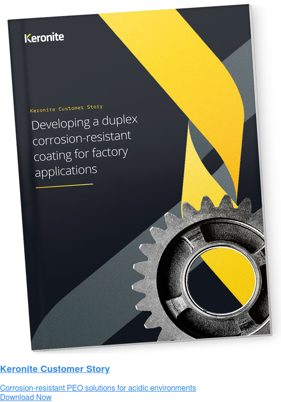
Additional chemical resistance can be achieved through the addition of a fluorocarbon-based duplex layer or sealer. The PEO coating can offer a rough adhesive surface for the fluoropolymer coating to bind with. The underlying PEO coating provides additional mechanical strength and stress crack resistance, while the fluoropolymer gives the ultra-clean, chemically resistant surface.
For more information about PEO coatings and how they can benefit manufacturing equipment in the semiconductor industry, get in touch. Our experienced team of materials scientists can develop custom coatings for aluminium, designed to withstand the extreme conditions of semiconductor fabrication.

 Keronite is now part of the CWST engineered coatings business.